
| Home | S-100 Boards | History | New Boards | Software | Boards For Sale |
| Forum | Other Web Sites | News | Index |
 |
|
 |
 |
 |
 |
 |
 |
 |
 |
|
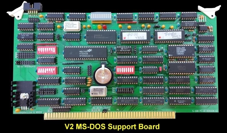
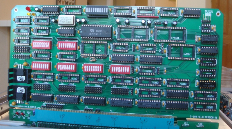
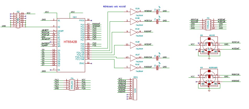
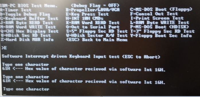
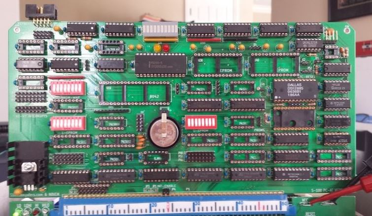
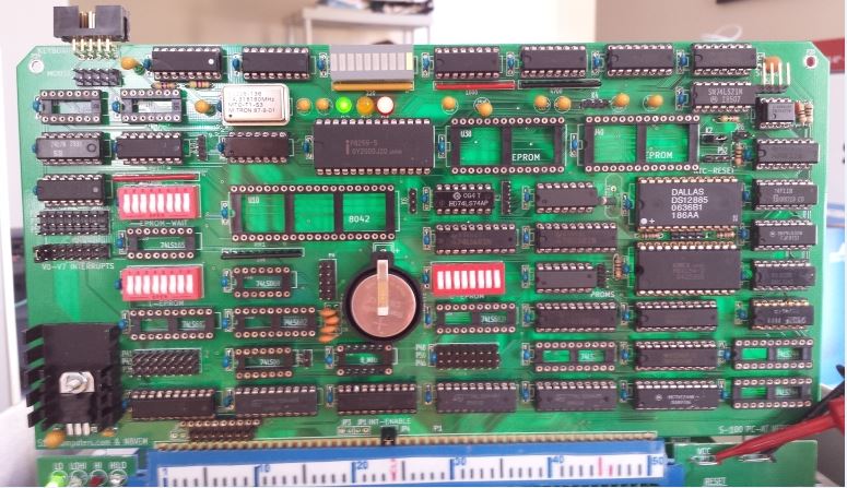
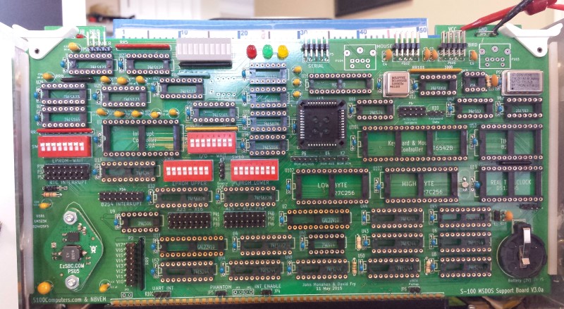
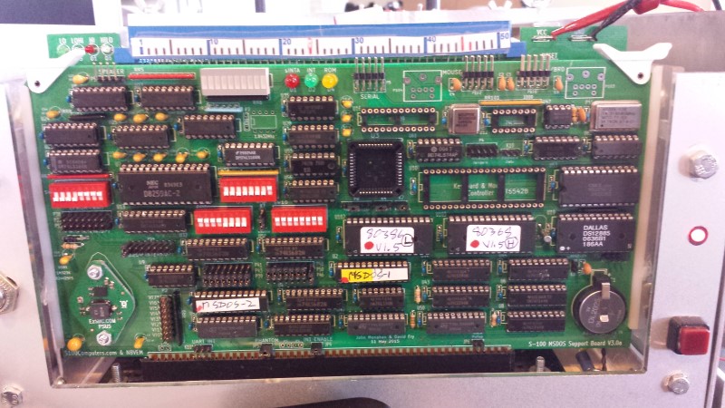
| 1. | Add a HolTek HT6542 PC keyboard controller chip to allow a MSDOS keyboard and mouse connection | |
| 2. | Replace the RTC with a chip that utilizes a separate battery for future replacements/availability | |
| 3. | Optimize the board layout and traces so the overall lengths are shorter and more reliable | |
| 4. | Remove the S100 bus extra wait state circuit | |
| 5. | Label the jumper options on the board better |
 |
 |
 |
 |
 |
 |
|
|
 |
 |
 |
 |
 |
 |
 |
 |
 |
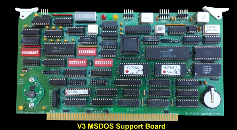
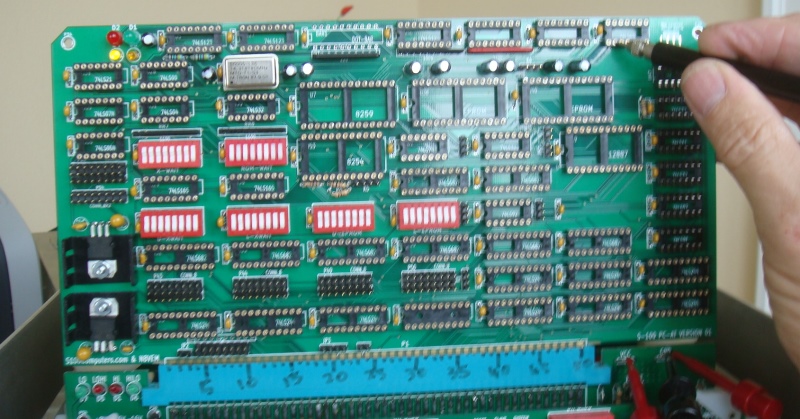
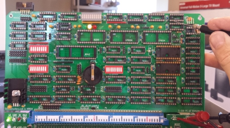
| 1. | Added two 22V10 GALs for board port decoding. | |
| 2. | Add an AT compatible 16550 UART and RS232 driver and port connection | |
| 3. | Optimize the 8258A Interrupt controller circuit and add a wait state generator (0-8 wait states for INTAs) | |
| 4. | Correct errors on the AT compatible Timer sound/speaker output. (Ports, jumpers) | |
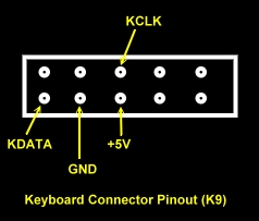
| 5 | Added PC style PS/2 mini-DIN connectors for the keyboard and mouse connectors. | |
| 6. | Add three options for the 5V regulator. A TO-3 LM323K, an EzSBC PSU5 or a Pololu 3A switching regulator. | |
| 7. | Hand lay down the Vcc line for efficient power distribution on the board. | |
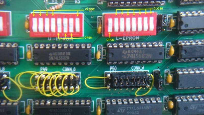
| 8. | Corrected silk screen labeling of Upper/lower EPROM switches (SW6 & SW10) | |
| 8. | Silk screen labeled all IC's for easier assembly/debugging. |
|
|
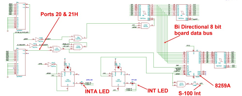
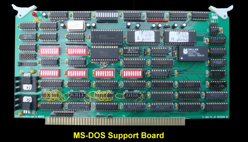
To understand how the two GALs have been spliced into this V3 board you should open up the schematic of the V2 MSDOS board
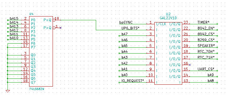
The first GAL U2, provides decoding for all of the I/O ports used by the various sections of this V3 MSDOS Support board. The GAL programming code is provided below but here is the relevant Equations Section:-
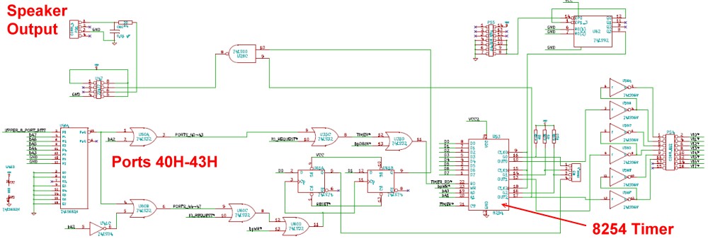
/TIMER = /UP6_BITS * /bA9 * /bA8 * /bA7 * bA6 * /bA5 * /bA4 * /bA3 * /bA2 * /IO_REQUEST
There are not enough input pins on this GAL for all the 16 I/O port address lines. We set the upper 6 address lines with the 74LS682 comparator U4.
Here is the relevant circuit:-
 |
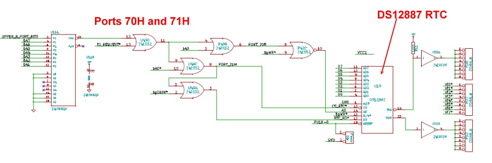
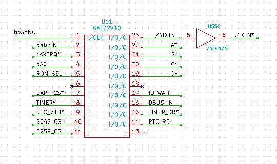
Some of the output pins of this GAL feed directly into the second GAL (U11) to directly address the Timer ( U53) and RTC (U19) chips.
 |
I/O port
addressing for the Timer D8254 registers (U53)
and the D-Type flip flops
that control the Timer 2 gate for speaker sound are now generated by the GAL
ffixed
I/O port decoder. The speaker port address has also been updated to port 61H as
per PC XT/AT spec.
I/O Ports
40H to 43H & Port 61H
/TIMER
= /UP6_BITS * /bA9 * /bA8 * /bA7 * bA6 * /bA5
/SPEAKER = /UP6_BITS * /bA9 * /bA8 * /bA7 * bA6 * bA5
*
/bA4 * /bA3 * /bA2 * /bA1 * bA0 * /IO_REQUEST
The TIMER_RD* signal is also generated in this second GAL (U11) by taking the signal TIMER* from GAL U2 and applying the following equation, this replaces U35D in the V2 schematic.
TIMER_RD = TIMER + /bpDBIN
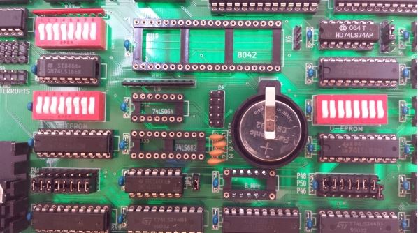
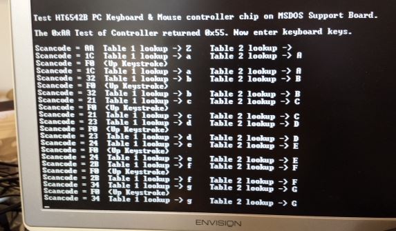
There has been no change to the 8042 style Keyboard/Mouse controller from the V2 schematic, except that the 8042_CS* chip select signal is now generated by the fixed address port decoder of GAL U2. The equation element /8042_EN below is a status input set by an external jumper to permit enable/disable the controller.
/8042_CS = /UP6_BITS * /bA9 * /bA8 * /bA7 * bA6 * bA5 * /bA4 * /bA3 * /bA1 * /bA0 * /IO_REQUEST * /8042_EN
In the RTC section (U19) of the V2 schematic four ‘OR’ gates and one magnitude comparator have been removed and replaced by two equations in GAL U2:-
/RTC_70H = /UP6_BITS * /bA9 * /bA8 * /bA7 * bA6 * bA5 * bA4 * /bA3 * /bA2 * /bA1 * /bA0 * /IO_REQUEST
/RTC_71H = /UP6_BITS * /bA9 * /bA8 * /bA7 * bA6 * bA5 * bA4 * /bA3 * /bA2 * /bA1 * bA0 * /IO_REQUEST
and one equation in the glue logic GAL, GAL U11
RTC_RD = RTC_71H + /bpDBIN
With the extra new board
space available a new section
has been added to incorporate a PC style
16660 UART. Address bits bA9
and bA8 had to be brought into GAL U2 to enable port decoding of 3F8H
-- the normal COM1 PC Serial port. Aalternative
port addresses would
just
require changes to the /UART_CS
equation.
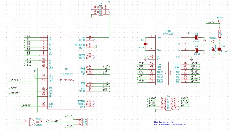 |
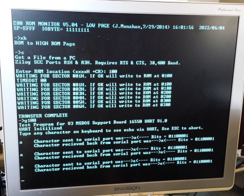
U16 and the connector P6 allow for a standard RS232 hookup. Please refer to our Serial I/O board for more help in this area if needed.
Receiving a little more modification from the V2 board, the 8259A interrupt controller circuit inverter U37D has been changed to a 74LS06 in a drive to reduce chip count. The D8259 chip select signal 8259_CS* is now generated inside GAL U2 with the equation:-
 |
 |
 |
|
|
 |
 |
 |
|
|
 |
 |
This page was last modified on 06/07/2023